Your Trusted Partner In Wafer Bumping and IC Packaging
Si-Craft Technologies provides specialized IC packaging and wafer bumping services, with a focus on prototyping and small- to mid-volume production. We support customers from concept to fully packaged, reliable devices, delivering flexible and high-quality solutions that meet evolving semiconductor requirements. Partner with Si-Craft Technologies for trusted expertise in wafer bumping, IC assembly, and custom package development.
Expert IC Packaging Solutions
At Silicon Craft Technologies, we specialize in tailored IC packaging and assembly services, guiding you from concept to reliable, high-quality devices for your semiconductor needs.


Prototyping Solutions
Assembly Prototyping & Custom Packages — Si-Craft Technologies supports proof-of-concept and custom package development for unique device requirements. We design and assemble custom ceramic or plastic packages, integrating tailored layouts, materials, and interconnect options. Ideal for early-stage validation and small-volume builds, our service bridges the gap between concept and full-scale production.
Small-Volume Production
Flexible low-quantity builds utilizing open cavity ceramic and selected plastic packages, ideal for prototype development, process validation, and pre-production runs. Si-Craft Technologies ensures full assembly support with production-grade materials and processes suited for evaluation and early-stage device integration.
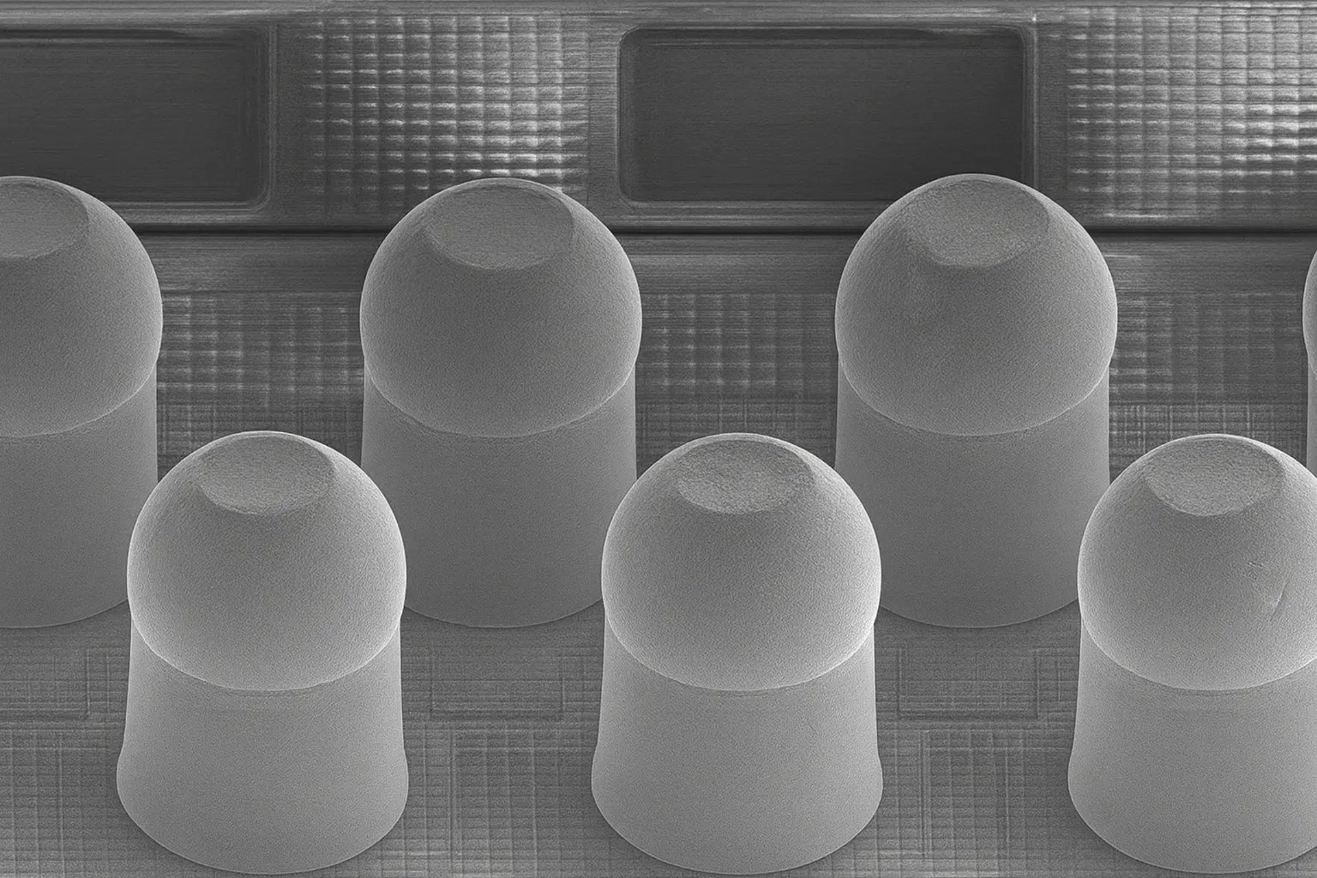
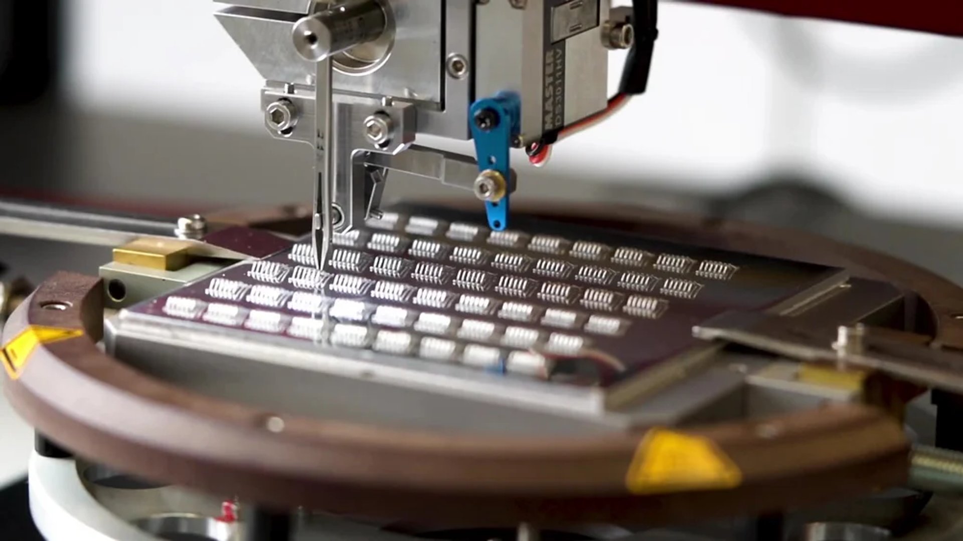
Small Volume Flip Chip and WLCSP Wafer Bumping
Offering advanced wafer-level bumping solutions, Si-Craft Technologies delivers reliable interconnect structures for flip-chip, WLCSP, and 3D IC packaging. Our capabilities cover electroplated solder, ENIG/ENEPIG, copper pillar, and stud bumping processes, supporting both lead-free and gold bump options. Each wafer undergoes precision under bump metallization (UBM) to ensure optimal adhesion, diffusion control, and solder wettability. Designed for prototype and small-volume production, our bumping services provide consistent bump height, fine-pitch accuracy, and excellent compatibility with open-cavity or custom package assemblies.
Our Product Range
Explore our advanced semiconductor products for various applications.
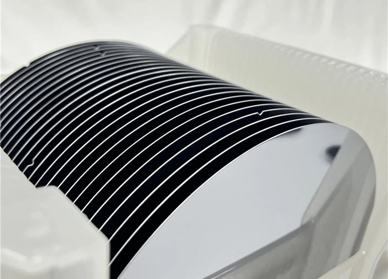
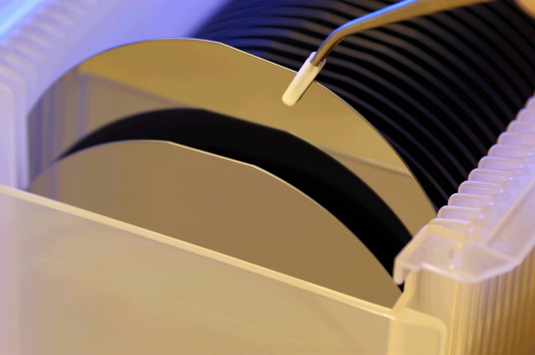
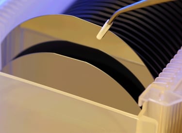
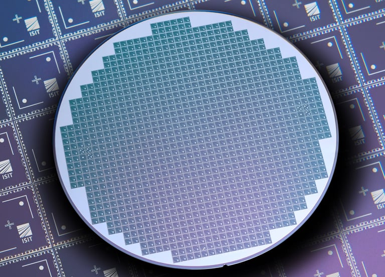
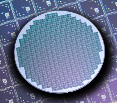
Bare Silicon, GaAs, GaN, InP, Sapphire, Glass, and Ceramic Wafers — substrates offered in various sizes and specifications for semiconductor, optoelectronic, MEMS, and advanced packaging applications.
Prime Silicon, GaAs, GaN, InP, Sapphire, Glass, and Ceramic Wafers — precision-engineered, low-defect, low partical count, substrates with tight TTV, surface roughness, and flatness control for device fabrication and advanced process development.
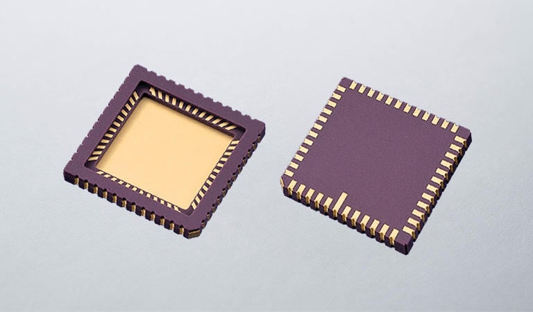
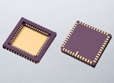
Open Cavity Packages
Open Cavity Packages (Ceramic & Plastic) — high-reliability NTK and Kyocera packages, available in various configurations for die attach, wire bonding, and hermetic or non-hermetic device assembly applications.
Bare Wafer
Prime Wafer
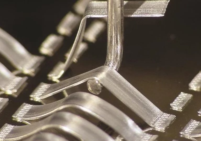
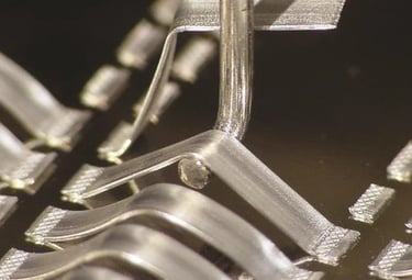
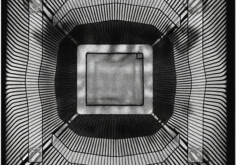
Daisy Chain
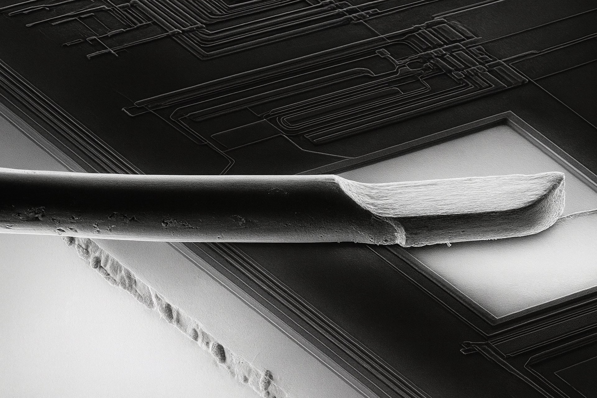
Bonding Wires
Epoxy
Test wafers - with interconnected metal routing designed to evaluate assembly integrity, solder joint reliability, and process performance under environmental stress. Ideal for failure analysis, drop and thermal cycling tests, and underfill evaluation, daisy chain structures provide simple pass/fail electrical continuity (0 Ω / ∞ Ω) measurements, enabling engineers to optimize bonding, reflow, and packaging processes.
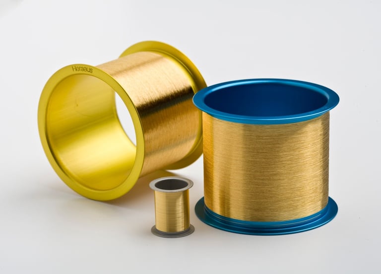
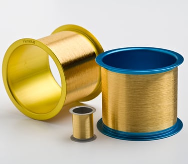
Bonding Wires (Au, Al, Cu) — high-purity Au (Gold), Al (Aluminum), and Cu (Copper) bonding wires supplied from leading manufacturers such as Tanaka, Heraeus, and Nippon Micrometal. Available in multiple diameters and finishes for ball, wedge, and ribbon bonding, these wires deliver superior conductivity, bond strength, and long-term reliability for semiconductor, power, and optoelectronic packaging applications.
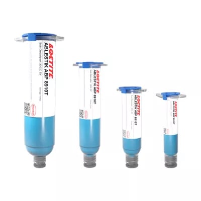
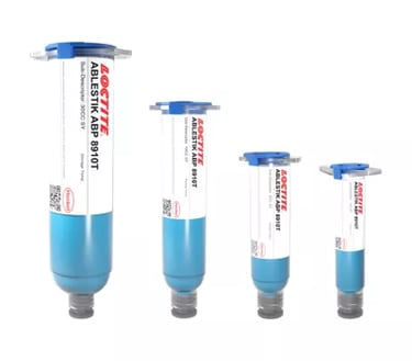
Die Attach Epoxy (B-Stage, Filled & Anisotropic Types) — high-performance epoxy adhesives from Loctite / Henkel, Master Bond, and DELO, designed for semiconductor and optoelectronic packaging. Available in B-stage, thermally filled, compliant, and anisotropic conductive formulations, these materials offer reliable adhesion, stable cure profiles, and excellent thermal and mechanical performance for diverse die attach applications.
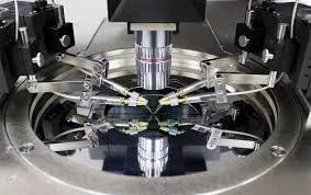
Failure Analysis and Reliablity Services
Comprehensive Failure Analysis and Reliability Testing services ensuring structural integrity, electrical performance, and long-term reliability of semiconductor packages using advanced analytical, mechanical, and environmental methods.
Analytical & Imaging
Advanced imaging and compositional analysis tools identify structural defects, contamination, and material inconsistencies using SEM, EDX, X-ray, XRF, SAM, and decapsulation techniques.
Mechanical & Physical Evaluation
Mechanical inspection and stress analysis through cross-sectioning, thermal hotspot mapping, and visual inspection to verify internal structure, bonding integrity, and physical package robustness.
Continuity and functional electrical evaluations ensure device integrity, performance consistency, and fault isolation before and after environmental or reliability stress conditions.
Electrical & Functional