
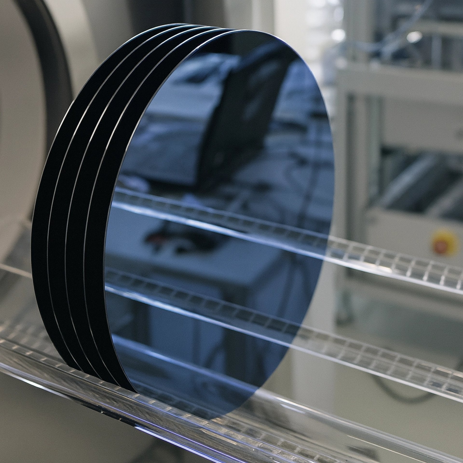
Wafer Backside Metallization (BSM)
Si-Craft Technologies provides precision wafer backside metallization (BSM) services engineered for power, RF, and MEMS devices. Our process integrates advanced surface preparation, adhesion layer engineering, diffusion barrier control, and solderable finishing to deliver reliable die attach and superior thermal management. Each BSM stack is customized for wafer material, device requirements, and downstream assembly — ensuring optimal electrical, mechanical, and thermal performance across Silicon, SiC, GaN, and compound substrates.
Our Backside Metallization Capabilities
Backside metallization is performed after device fabrication and thinning, creating a conductive, solderable surface tailored to each wafer material and bonding method. Si-Craft’s proprietary metal stack design controls diffusion, adhesion, and stress to meet stringent mechanical and thermal reliability requirements across different attach systems such as eutectic AuSn, Ag sintering, and Pb-free solder.
ElectroPlating
Write a short text about your service. Highlight key benefits for potential clients.


PVD
Write a short text about your service. Highlight key benefits for potential clients.


Metal Stack Design by Wafer Material
BSM Attach Compatibility
Si-Craft’s backside metallization supports Au-based eutectic bonding, Ag sintering, Pb-free solder, and conductive epoxy attach.
Metal stacks are optimized for wetting behavior, thermal conductivity, and mechanical stress control — ensuring consistent die shear strength and thermal cycling reliability across all attach processes.
Each wafer undergoes comprehensive thickness mapping, adhesion testing, and electrical continuity checks.
Our barrier engineering ensures zero interdiffusion during high-temperature attach cycles, while protective capping layers (Ni/Au or Ni/Ag) maintain solderability and corrosion resistance during long-term storage.
Reliability and Quality Assurance
Custom BSM Stack Engineering
Every device family has unique stress, diffusion, and attach temperature limits.
Si-Craft’s process engineers work directly with your design team to define metal thickness, stress control, and diffusion barrier strategy specific to your wafer and assembly flow. Contact us to discuss custom metallization stacks and evaluate thermal/electrical performance trade-offs for your next build.
Partner with Si-Craft Technologies for precision backside metallization that enhances die attach strength, thermal conductivity, and long-term package reliability.
Our process flexibility covers everything from prototyping to mid-volume production, ensuring every wafer meets the highest back-end manufacturing standards.
Get in Touch
Our team will review your request and respond with a within 1-3 business days via email
Contact
+65
Sales@Si-CraftTechnologies.com