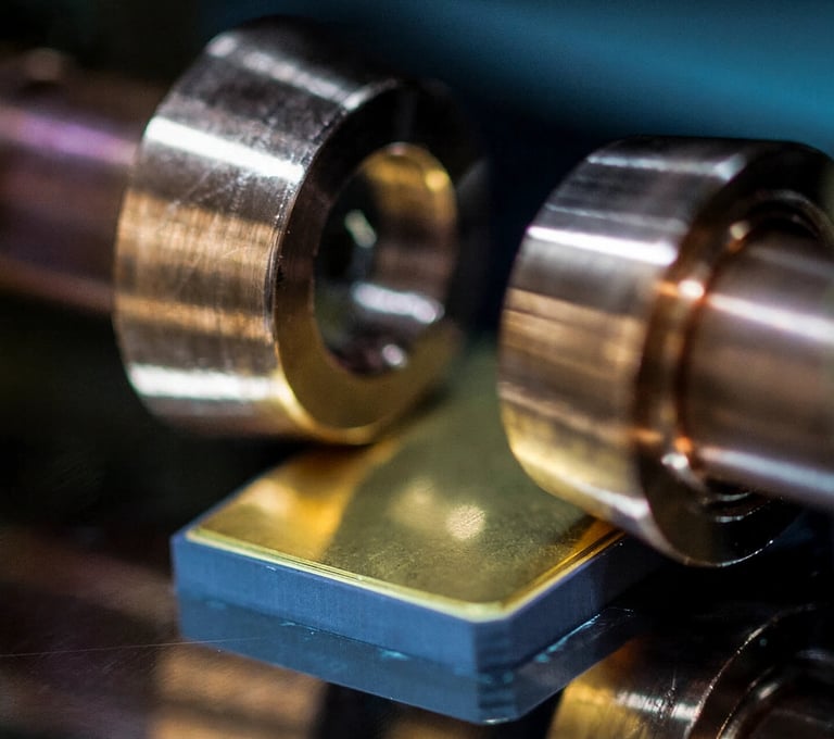

Package Assembly
Si-Craft Technologies provides complete semiconductor package assembly solutions — from wafer backgrinding and precision dicing to die attach, wire bonding, die sorting, and hermetic sealing. Our process chain ensures mechanical integrity, electrical reliability, and long-term device performance. With expertise in Si, GaAs, and advanced materials, Si-Craft delivers production-ready assembly support for hybrid, RF, and optoelectronic packages with uncompromising precision and process control.
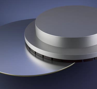
Wafer Backgring Services offered by Si-Craft
Precision thinning of wafers to final target thickness for assembly integration.
Uses high-rigidity spindle grinders ensuring low total thickness variation (TTV).
Controlled removal rates to maintain wafer planarity and surface integrity.
Process optimized for Si, GaAs, SiC, and compound semiconductor wafers.
In-process measurement ensures consistent die strength and warp control.
Optional two-step coarse/fine grind for reduced surface stress.
Minimal subsurface damage through fine-grit finishing wheels.
Post-grind cleaning and tape removal performed in a clean environment.
Supports ultra-thin wafers (<100 µm) for advanced packaging.
Suitable for subsequent dicing, die attach, and wire bonding operations.
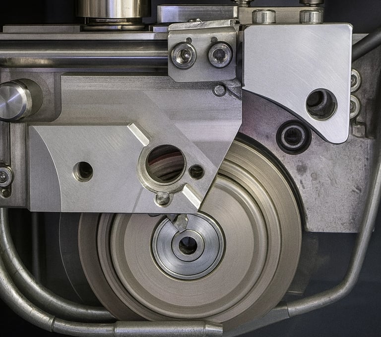
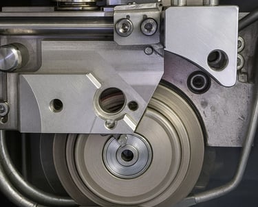
Wafer Dicing Services Offered by Si-Craft
Precision singulation of processed wafers into individual dies.
Utilizes high-speed dicing saws with micron-level accuracy.
Blade selection optimized for material hardness and kerf width.
Controlled coolant flow prevents edge chipping and thermal shock.
Compatible with Si, GaAs, GaN, InP, and ceramic substrates.
Optical alignment ensures accurate cut-to-pattern registration.
Taper and burr control for high-yield die separation.
Optional stealth laser dicing for ultra-thin or brittle wafers.
Process data logged for traceability and lot tracking.
Prepared dies mounted on UV-release or thermal-release film.
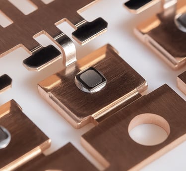
Die Attach Services offered by Si-Craft
Precision thinning of wafers to final target thickness for assembly integration.
Uses high-rigidity spindle grinders ensuring low total thickness variation (TTV).
Controlled removal rates to maintain wafer planarity and surface integrity.
Process optimized for Si, GaAs, SiC, and compound semiconductor wafers.
In-process measurement ensures consistent die strength and warp control.
Optional two-step coarse/fine grind for reduced surface stress.
Minimal subsurface damage through fine-grit finishing wheels.
Post-grind cleaning and tape removal performed in a clean environment.
Supports ultra-thin wafers (<100 µm) for advanced packaging.
Suitable for subsequent dicing, die attach, and wire bonding operations.
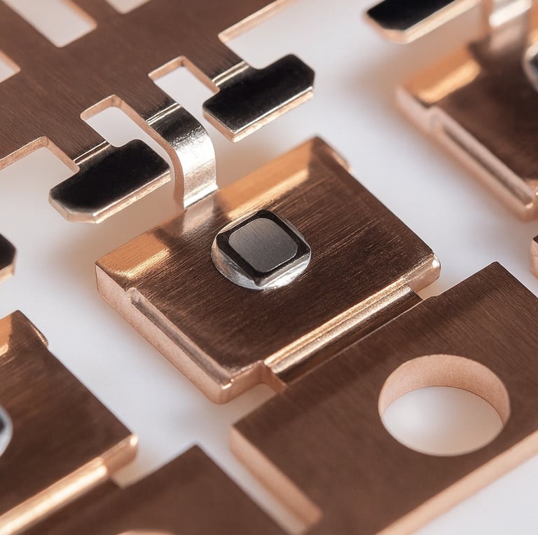
Wire Bonding Services Offered by Si-Craft
Fine-pitch interconnection using Au, Al, or Cu bonding wire.
Capable of thermosonic, ultrasonic, and thermocompression bonding.
Optimized for both wedge and ball bonding geometries.
Maintains precise loop height and wire sweep control.
Bond pull and shear testing ensure bond reliability.
Compatible with die sizes from sub-mm to large power devices.
Programmable bond parameters for multi-device flexibility.
Process conducted in temperature-controlled clean area.
Real-time monitoring of ultrasonic power and bonding force.
Designed for RF, high-frequency, and power device applications.


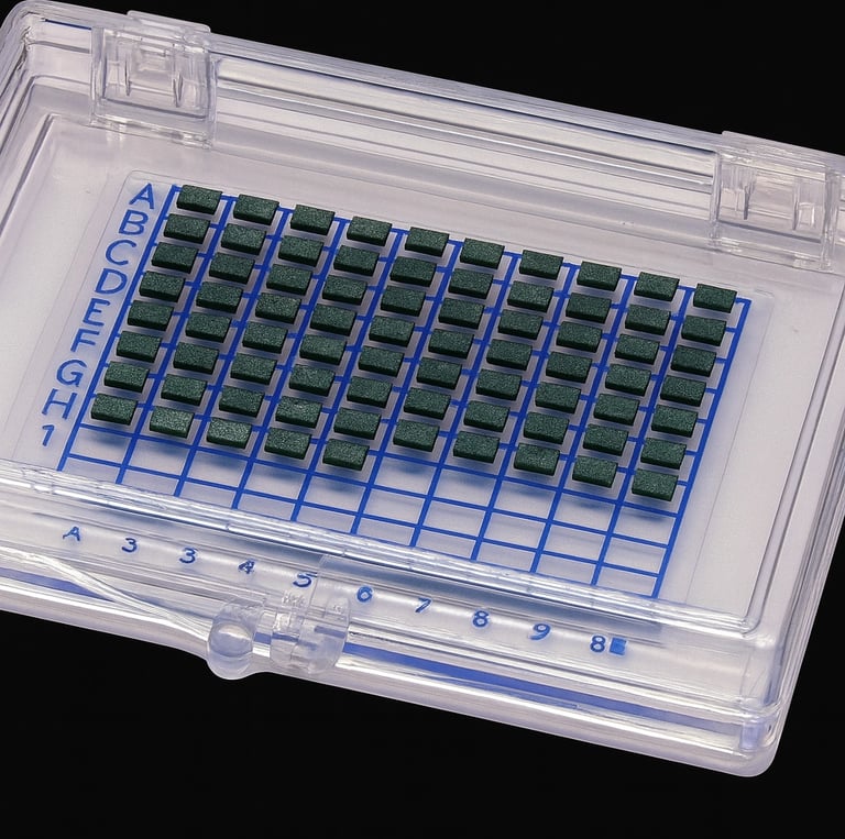
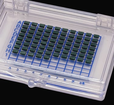
Die Sorting Services offerd by Si-Craft
Post-test die sorting using automated vision inspection systems.
Classifies dies by electrical bin or visual defect criteria.
Integrated mapping with wafer-level test data.
Gentle vacuum or collet pick-up prevents mechanical damage.
Supports waffle pack, gel pack, or tape-and-reel output.
Cleanroom-controlled environment minimizes contamination.
Die traceability maintained through barcode or 2D ID.
Configurable sorting rules for multi-lot flexibility.
High throughput compatible with 4–12 inch wafer formats.
Ready for direct feed into assembly or hermetic packaging.
Hermetic Sealing, Lid Assembly Services offerd by Si-Craft
Seam AuSn solder sealing ensures hermetic package integrity.
Kovar™ lids and thick-film seal rings plated with Ni/Au.
Uses resistance seam welding with conical electrodes.
No forming gas required; inert environment optional.
80Au20Sn eutectic solder provides high strength and low voids.
Gravity-fit alignment eliminates complex fixturing.
Ideal for hybrid circuits, sensors, and optoelectronic packages.
Visual seam observation ensures process quality.
Final helium leak testing per MIL-STD-883 standards.
Proven long-term hermeticity and corrosion resistance.