Wafer Bumping
Delivering precision-engineered wafer bumping solutions, Si-Craft Technologies enables advanced interconnect structures for flip-chip, WLCSP, and 3D IC applications. Our processes support a full range of bumping methods — including electroplated solder, ENIG/ENEPIG, copper pillar, and gold stud bumping — designed to meet diverse electrical, thermal, and mechanical performance requirements. Each wafer undergoes carefully optimized under bump metallization (UBM) to ensure strong adhesion, diffusion control, and solder reliability. Focused on prototype and small- to mid-volume production, our bumping services deliver fine-pitch accuracy, consistent bump uniformity, and compatibility with custom or open-cavity packages, providing the foundation for reliable next-generation semiconductor assemblies.
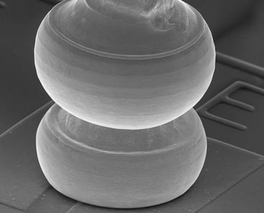
Electroplated Solder Bumps
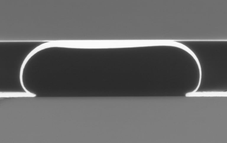
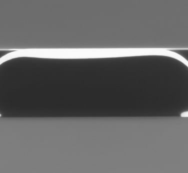
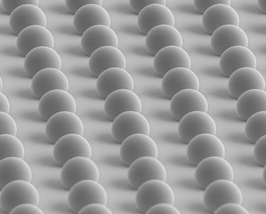
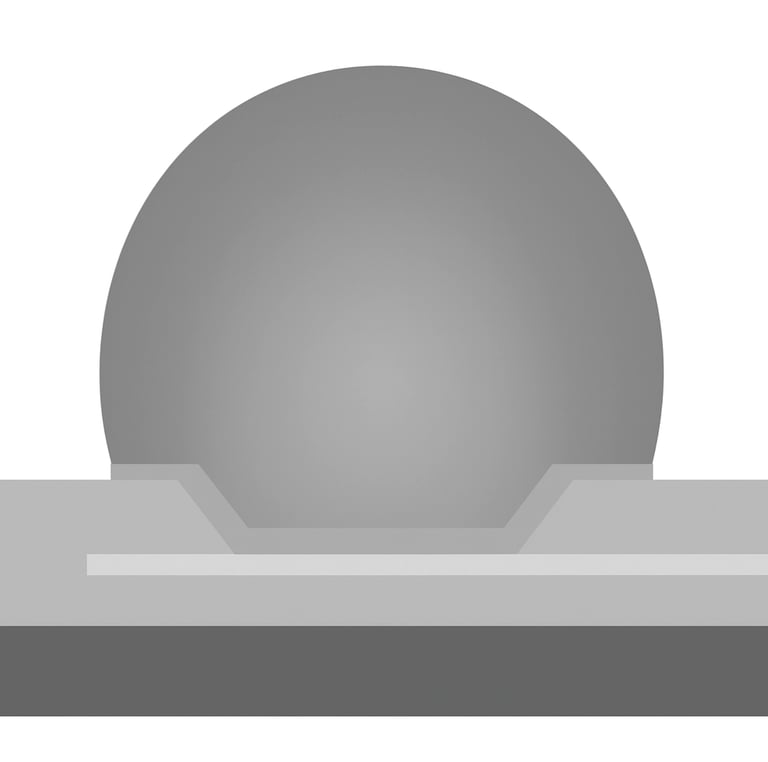
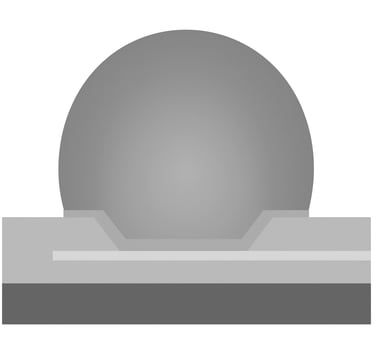
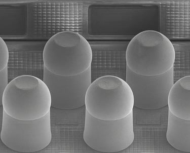
Electroplated solder bumps are a proven and established interconnect technology for fine-pitch flip-chip and wafer-level packaging. The process flow consists of photoresist patterning, UBM deposition, solder electroplating, resist stripping, and reflow. During reflow, the plated solder forms uniform dome-shaped bumps through controlled surface tension.
Lead-free alloys such as Sn–Ag and Sn–Ag–Cu (SAC) are standard, with eutectic Sn–Pb used in legacy applications. For specialized requirements, Au or Au–Sn plating is implemented. Typical UBM stacks—Ti/Cu/Ni/Au or TiW/Cu/Ni/Au—provide strong adhesion, an effective diffusion barrier, and excellent solder wetting characteristics.
Bump heights range from 25 to 100 µm, with diameters around 30 µm for fine pitch, and pitches down to 40–50 µm or lower in advanced nodes. Electroplating ensures tight control over bump height, volume, and placement, supporting high-yield, wafer-level batch processing. Process uniformity is maintained through optimized current distribution and well-controlled plating parameters. Electromigration reliability, voiding behavior, and wetting are governed by solder volume, pad design, and UBM integrity. This method consistently delivers high-performance, fine-pitch interconnects suitable for advanced packaging roadmaps.
Electroless Ni / Au (ENIG) / ENEPIG / Electroless UBM & Solder
Electroless UBM processes use chemical Ni(P) deposition followed by immersion Au, sometimes with an intermediate Pd layer (ENEPIG). No external current is required, simplifying processing and enhancing coverage uniformity. Solder is then deposited—by plating, paste, or drop—and reflowed to form bumps. Typical Ni(P) thickness is a few micrometers, while Au thickness ranges from tens to hundreds of angstroms.
Bump dimensions typically range from 10 µm to 40 µm, suitable for WLCSP, MEMS, RF, and sensor devices. Shapes are small domes or flats, with tight pitches achievable. Uniform Ni and Au thickness is essential for controlling intermetallic formation and ensuring adhesion reliability. Step coverage over nonplanar surfaces requires careful process optimization. This low-cost, well-controlled UBM and bumping method is widely used for moderate bump sizes and tight-pitch packaging.
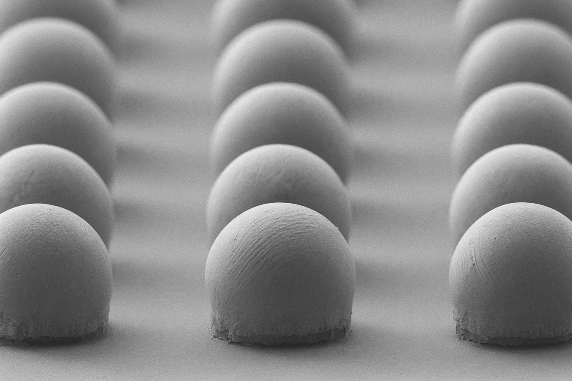
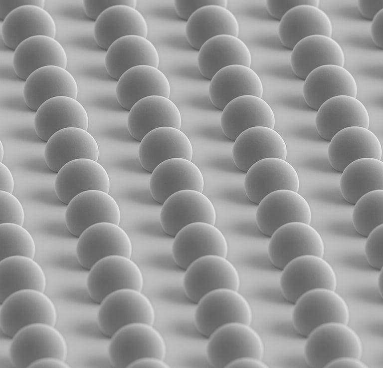
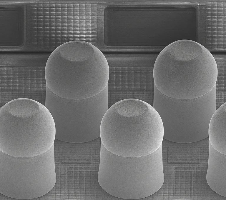
Copper Pillar Bumps (Cu Pillar / Microbumps with Solder Cap)
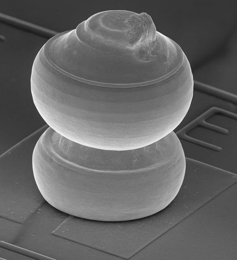
Copper pillar bumps are a proven interconnect solution for high-density flip-chip, 2.5D/3D IC, and fine-pitch packaging. The process plates a rigid copper column, adds a thin solder cap, and reflows to form a controlled fillet. Unlike solder bumps, Cu pillars retain standoff height, ensuring stable joint geometry.
The pillar is copper with a Sn–Ag or Sn–Ag–Cu solder cap. A UBM stack (e.g., Ti/Cu seed/Ni barrier/Cu) and Ni barrier layer control adhesion and intermetallic growth. Typical pillar diameters are 20–50 µm, heights 40–100 µm, with solder caps a few micrometers thick. Pitches under 130 µm are common, with advanced designs going finer.
This structure offers excellent thermal and electrical performance, dimensional control, and reliability. Critical factors include lithography limits, resist aspect ratio, coplanarity, stress, and intermetallic formation. Cu pillar technology is established for advanced packaging requiring tight pitch and robust interconnects.
Solder Ball / Pre-formed Ball Placement /
Paste Printing Bump
Solder ball and paste printing bumping are standard methods for large-pitch flip-chip and WLP/BGA packages. The process places pre-formed solder balls (ball drop) or printed solder paste on UBM pads, followed by reflow to form spherical bumps. UBM is deposited first, then solder is applied on top.
Common solder materials include Sn–Ag, Sn–Ag–Cu, and low-melt alloys like Sn–Bi. Typical UBM stacks are Ni/Au or Ti/Cu/Ni/Au. Ball sizes typically range from 100 to 500 µm or more, with bump height close to the original ball diameter after reflow. This method is optimized for coarser pitches, not ultra-fine geometries.
The process is simple, mature, and cost-effective for large-pitch interconnects. However, fine-pitch use is limited by ball size, alignment accuracy, stencil constraints, and void control. For small geometries, solder distribution and uniformity become challenging.
Stud Bumping
Stud bumping uses a wire bonder to form a molten ball at the wire tip (Au, Cu), bond it to the pad, then break the wire to leave a bump. This technique is common in R&D, prototyping, and small-volume fine-pitch applications where wafer-scale plating is not justified.
Typical ball diameters range from 15–35 µm, forming semi-spherical or “nail-head” shapes after bonding. Pitch is determined by bonder precision and is generally coarser than advanced wafer-level processes. Pads often have Ni/Au or similar metallization to enhance bonding.
Stud bumping enables flexible, low-volume bumping without masks or plating steps. However, it has limitations in coplanarity, uniformity, and throughput due to its serial nature. It is effective for test vehicles and development builds but not practical for large production arrays.
Conductive Polymer / Adhesive Bump (Polymer Bumping)
Polymer bumping uses a conductive adhesive—typically an epoxy filled with silver flakes or metallic particles—dispensed or printed onto UBM pads and then cured. Some variants use anisotropic conductive adhesives (ACA), forming electrical connections only at the bump contact points. UBM is typically Ni/Au or Ti/Cu to ensure good contact and wetting.
Typical bump heights range from 25 to 100 µm, with dome or truncated dome profiles depending on dispensing. This method suits moderate pitches but is limited for ultra-fine geometries due to adhesive viscosity and print resolution.
Polymer bumps offer low-temperature processing and compatibility with flexible substrates, sensor arrays, RF, and MEMS applications where solder is unsuitable. However, their electrical and mechanical reliability is lower than metal bumps, with potential issues in conductivity stability, thermal cycling, and fatigue. Robust interface design is essential to maintain low contact resistance over time.