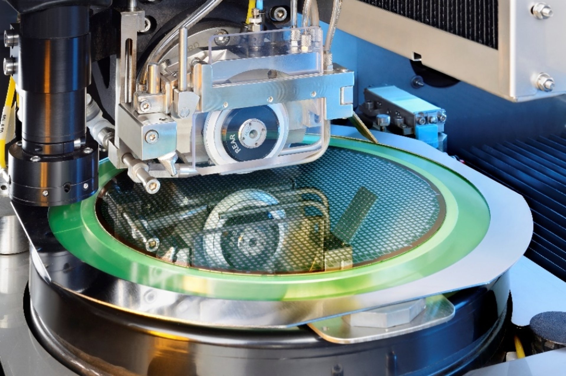
Wafer Dicing
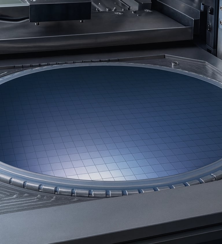
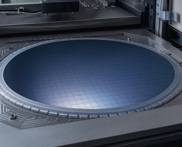
At Si-Craft Technologies, our dicing process is optimized for high-precision cutting across a range of materials including silicon, GaAs, GaN, InP, glass, and ceramic wafers. We utilize DISCO dicing blades and fully automatic dicing saws to achieve clean, consistent cuts with minimal chipping and particle generation. The process supports wafers up to 12 inches, maintaining tight kerf control and die placement accuracy within a few microns. Each recipe is tuned to the wafer’s thickness and material characteristics, ensuring smooth sidewalls, low edge damage, and reliable die separation ready for downstream packaging and assembly. Take a look below for full list of dicing services we offer here at
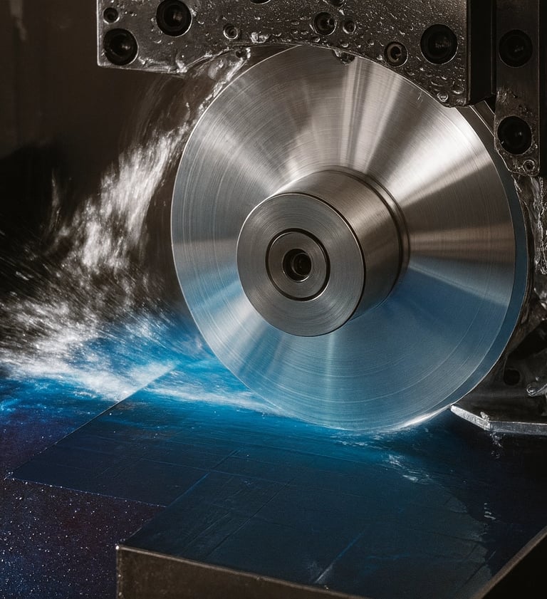
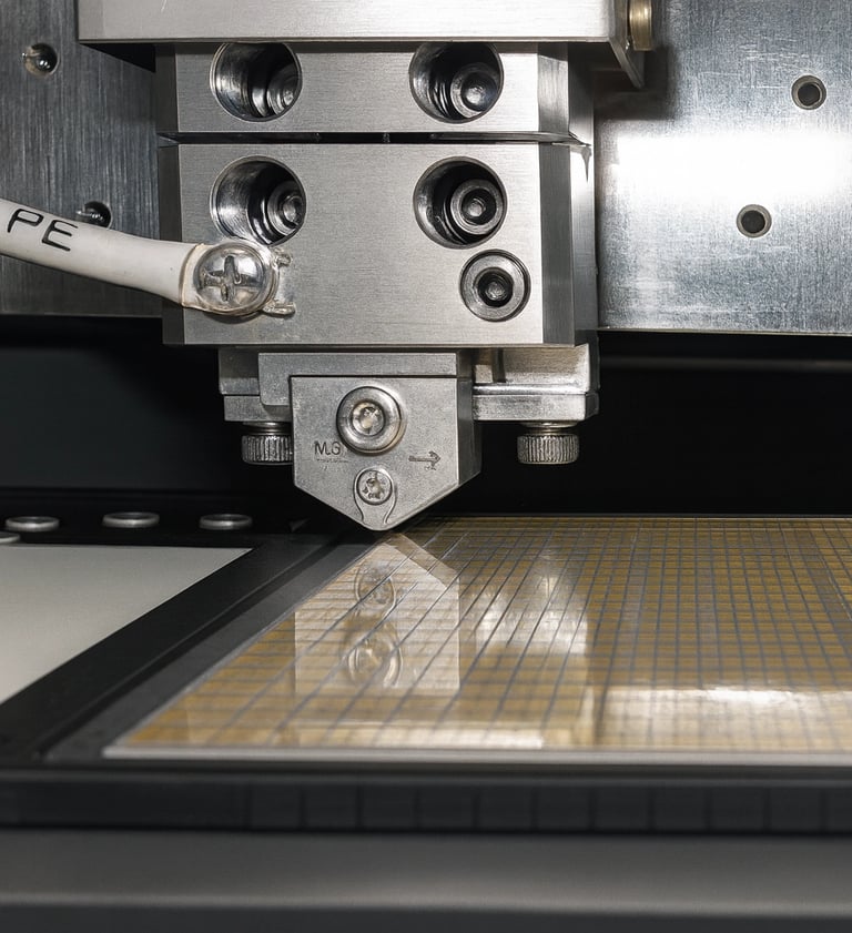
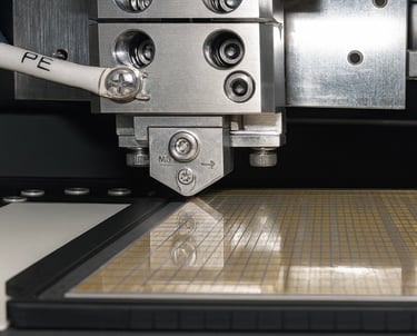
Mechnical Dicing (Saw Dicing)
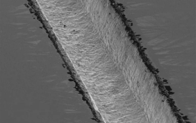
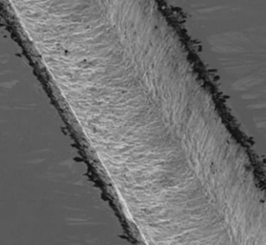
Mechanical dicing employs a high-precision spindle-mounted diamond blade to physically saw wafers along scribe lines. The process uses deionized (DI) water for cooling and debris removal, while spindle speed, feed rate, and blade grit size determine cut quality. This method remains the industry standard for silicon and compound wafers up to several hundred micrometers thick. While cost-efficient and high-throughput, it introduces mechanical stress, potential chipping, and kerf loss due to blade width. Optimization of blade wear, cut depth control, and chuck vacuum uniformity are essential for achieving tight die-edge integrity and maintaining device yield in high-volume production.
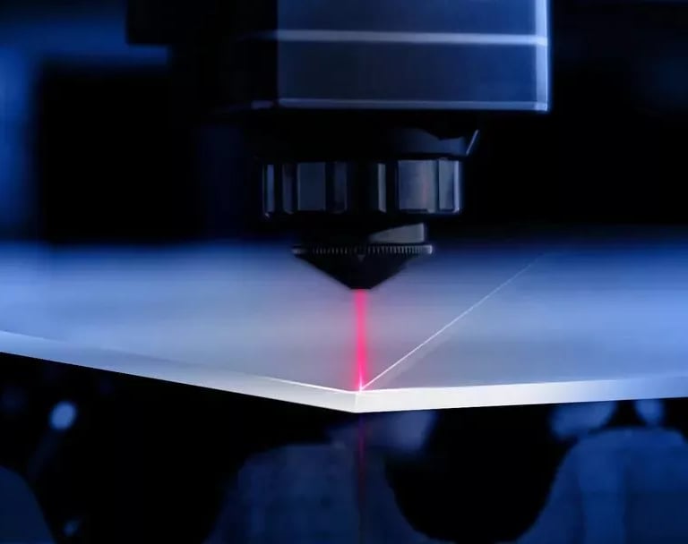
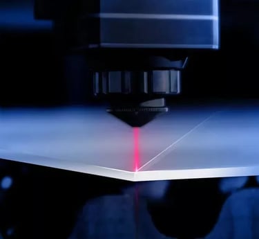
Stealth Dicing
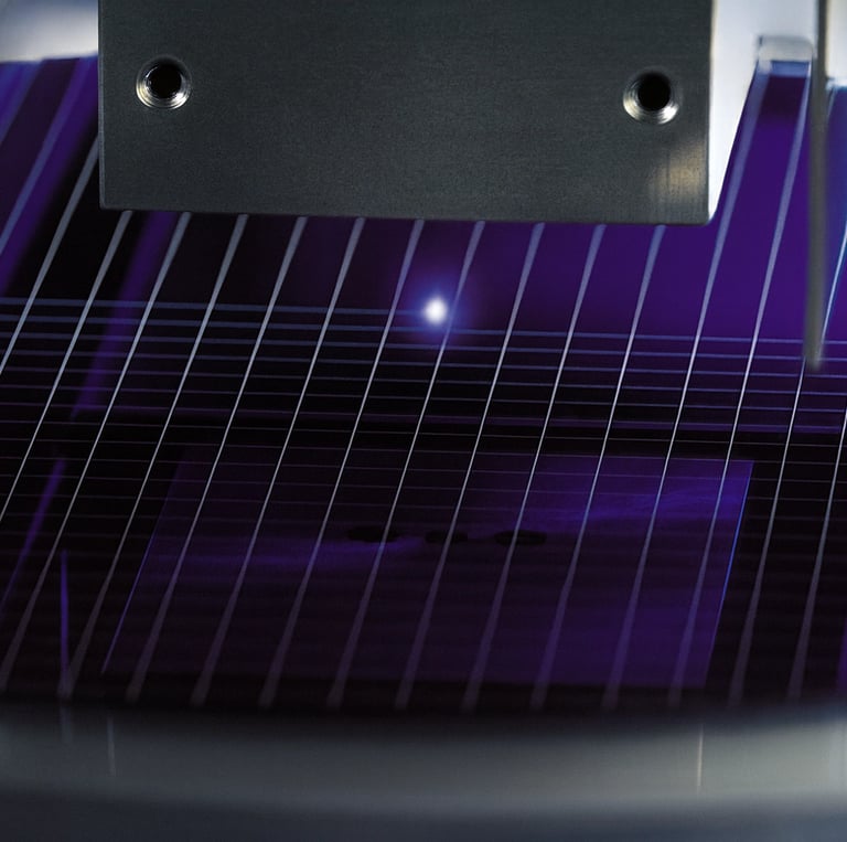
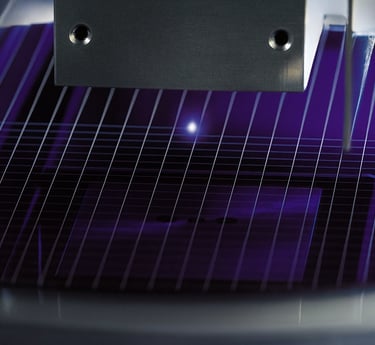
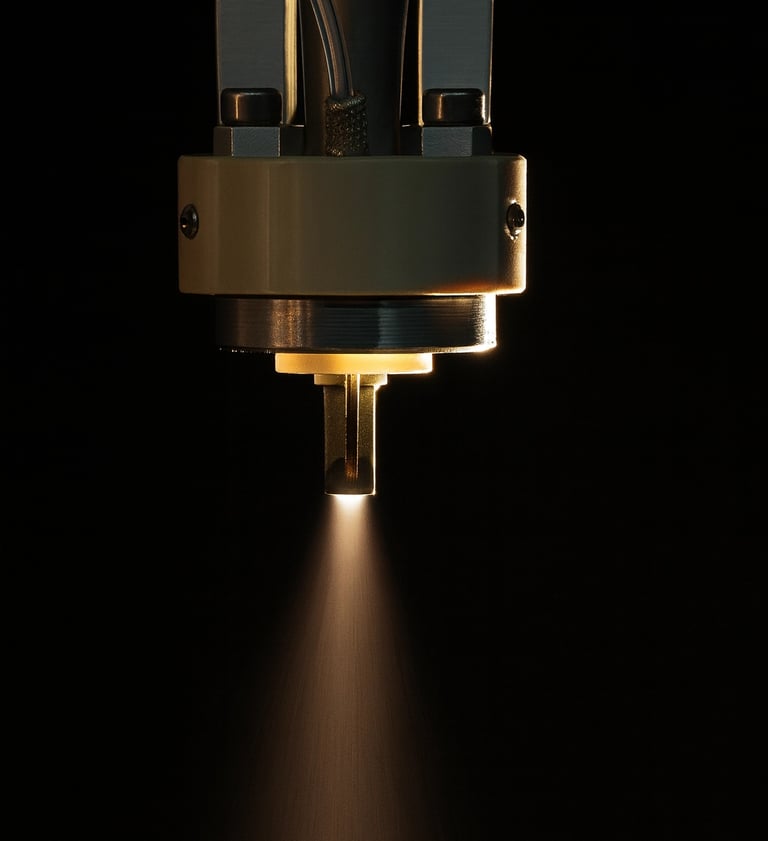
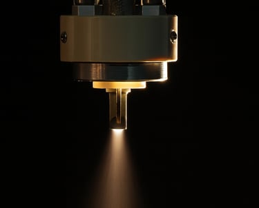
Stealth dicing employs a tightly focused near-infrared laser to create modified subsurface layers within the wafer volume. The laser forms localized micro-cracks that define controlled fracture planes beneath the surface. Wafer separation is achieved through expansion or stress application along these internal modification zones. The process eliminates kerf loss and surface contamination while preserving mechanical stability during dicing. Si-Craft’s stealth dicing systems deliver consistent internal layer formation with precise control over pulse energy, wavelength, and focal depth. The result is mirror-finish sidewalls, minimal debris, and superior die strength suitable for 3D integration and ultra-thin wafer singulation.
Dice-Before-Grinding (DBG)
The DBG process integrates dicing and thinning to enhance mechanical stability during wafer singulation. Shallow grooves are sawn into the wafer front-side streets prior to thinning. The wafer is then bonded to a carrier and ground from the backside until complete separation occurs along the pre-cut grooves. This controlled process maintains wafer rigidity, eliminates tape expansion, and prevents die breakage in ultra-thin device fabrication below 100 µm. Si-Craft executes DBG with precise depth calibration, stable grinding uniformity, and optimized bonding materials. The technique delivers exceptional die planarity and alignment accuracy for stacked and high-density package structures.
Hybrid Dicing
Hybrid dicing combines laser, mechanical, and plasma processes to optimize quality, throughput, and cost efficiency. Laser pre-treatment weakens dicing streets, followed by mechanical or plasma completion to achieve smooth and debris-free separation. This synergy minimizes chipping, reduces cutting force, and allows narrow street designs for maximum die count. Si-Craft custom-configures hybrid dicing sequences based on wafer thickness, metallization, and substrate type. The process provides superior edge definition and dimensional control for complex multilayer wafers and heterogeneous integration. Hybrid dicing enhances flexibility, ensuring optimal process selection for advanced packaging and system-in-package applications.
Plasma Dicing
Plasma dicing applies deep reactive ion etching (DRIE) or isotropic plasma etching to separate dies without any mechanical contact. After lithographically defining the dicing lanes with a photoresist mask, reactive gases such as SF₆ or O₂ plasma chemically etch the exposed silicon. The process delivers near-zero mechanical stress, ultra-smooth sidewalls, and the narrowest possible dicing lanes (<5 µm), improving die count per wafer. Plasma dicing is especially effective for thin, fragile wafers and for die-level packaging where cleanliness and debris control are critical. It enables advanced integration, wafer-level chip-scale packaging (WLCSP), and high-reliability MEMS device manufacturing.
Laser Dicing
Laser dicing utilizes tightly focused pulsed laser beams—often UV, green, or infrared wavelengths—to thermally ablate wafer material along narrow streets. The non-contact nature of the process eliminates mechanical stress and allows cutting of ultra-thin or brittle substrates such as SiC, GaAs, and glass. Advanced systems employ multiple laser modes, including direct ablation, scribing, and stealth modes, offering kerf widths below 10 µm. Beam positioning, pulse frequency, and energy density are precisely controlled for minimal heat-affected zones. Laser dicing achieves high die strength, exceptional edge quality, and scalability for complex wafer materials in advanced semiconductor packaging.
Scribe-and-Break
Scribe-and-break is a precision separation technique designed for brittle crystalline materials such as GaAs and glass. A diamond-tipped stylus or laser creates controlled scribe lines aligned to crystal orientation, initiating localized stress points. Mechanical force is then applied to propagate a clean fracture along these predefined paths. The method generates extremely narrow kerf widths and minimal particulate contamination. Si-Craft employs automated scribing equipment with high-accuracy force modulation to achieve uniform break propagation. This approach ensures high die strength, debris-free separation, and repeatable results across wafers where conventional blade or plasma dicing is impractical.
Frequently asked questions - Wafer Dicing
What is wafer dicing and why is it critical in semiconductor manufacturing?
Wafer dicing is the process of singulating processed semiconductor wafers into individual dies. It directly affects die strength, surface cleanliness, and yield. Si-Craft Technologies uses precision mechanical, laser, plasma, and hybrid dicing systems to ensure clean separations, minimal chipping, and maximum die integrity across all wafer materials.
How does Si-Craft ensure minimal chipping and edge damage?
Our process control integrates spindle load monitoring, vibration suppression, optimized feed rates, and DI water management. For non-contact processes like laser and plasma dicing, parameters are calibrated to eliminate thermal or plasma-induced microcracks. Post-dicing inspection verifies uniform die edges and zero particle contamination.
What wafer materials can Si-Craft dice?
Si-Craft supports a wide range of substrates including Silicon (Si), Gallium Arsenide (GaAs), Gallium Nitride (GaN), Silicon Carbide (SiC), Glass, Sapphire, and Compound Semiconductor wafers. Each material is processed using the most compatible dicing technology to maintain surface integrity and structural quality.
What wafer thicknesses can Si-Craft handle?
Si-Craft supports wafer singulation from 2mm down to ultra-thin wafers below 50 µm. Processes such as DBG, plasma, and stealth dicing are optimized for thin-wafer integrity and flatness preservation during backside thinning and die separation.
What dicing methods are available at Si-Craft Technologies?
We provide full-spectrum dicing solutions:
Mechanical Blade Dicing
Laser Dicing
Plasma Dicing
Stealth Dicing
Dice-Before-Grinding (DBG)
Scribe-and-Break
Hybrid Dicing
Each process is selected based on wafer thickness, device structure, and packaging requirements.
What are the advantages of plasma or stealth dicing over traditional blade sawing?
Plasma and stealth dicing eliminate mechanical contact, allowing sub-5 µm dicing lanes, no kerf loss, and higher die yield. These methods produce superior edge quality and are ideal for fragile or high-value wafers used in WLCSP and advanced packaging applications.
What information should customers provide when requesting a dicing quotation?
Please include wafer size, thickness, material type, street width, dicing pattern (saw map), and preferred singulation method if known. Our engineering team evaluates these parameters and provides a tailored dicing process and quotation.
Does Si-Craft offer wafer mounting and tape handling services?
Yes. Si-Craft provides UV and non-UV tape mounting, tape expansion, die sorting, and ring-frame handling. Mounting parameters are optimized to maintain alignment and prevent wafer warpage throughout the singulation and pick-and-place process.
How clean is the dicing process and what post-processing steps are included?
All dicing operations are performed under cleanroom conditions using filtered DI water. Post-dicing, wafers undergo cleaning, particle inspection, and drying in Class-100 environments. For plasma processes, dry etching ensures a debris-free surface without residue or ionic contamination.
How does Si-Craft verify dicing quality and yield?
Every wafer undergoes optical edge inspection, surface cleanliness assessment, and die-strength evaluation. Statistical process control (SPC) data and inspection reports are available upon request for traceability and quality assurance.
Can Si-Craft process wafers with metallization or passivation layers?
Yes. We apply controlled laser or plasma parameters that accommodate top metal layers, passivation films, or low-k dielectrics. Hybrid dicing is used for complex multilayer or backside-metallized wafers to maintain structural and electrical integrity.
Get in Touch
Our team will review your request and respond with a quotation within 1-3 business days via email
Contact
+1234567890
sales@Si-CraftTechnologies.com