
Analytical & Imaging
Precision imaging and material analysis form the foundation of accurate failure diagnostics. Using SEM, EDX, X-ray, XRF, SAM, and decapsulation, our team isolates structural defects, detects contamination, and characterizes material integrity across complex package architectures.
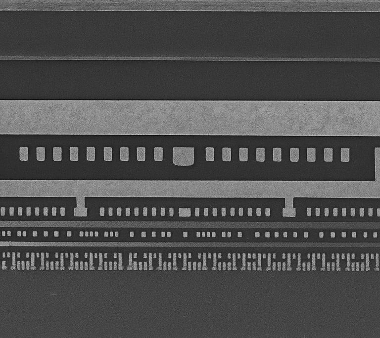
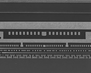
Scanning Electron Microscopy (SEM)
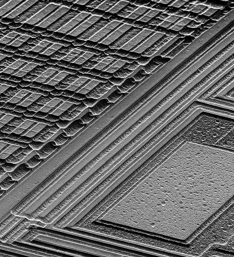
Scanning Electron Microscopy provides high-magnification, high-resolution imaging for detailed surface and structural analysis of semiconductor devices. It is a cornerstone tool in package failure analysis, enabling visualization of defects invisible to optical microscopy.
Reveals surface topography, grain structure, and fracture patterns.
Identifies process defects such as voids, delamination, and metal bridging.
Supports metallization integrity studies and bond interface evaluation.
Secondary Electron (SE) and Backscattered Electron (BSE) modes enhance material contrast and defect visibility.
When combined with Energy Dispersive X-ray Spectrometry (EDX), SEM offers both morphological and compositional information, critical for pinpointing contamination sources or process deviations at sub-micron scale.

Energy Dispersive X-ray Spectrometry (EDX)
EDX complements SEM by providing elemental analysis and material composition mapping within semiconductor packages and interconnects. It is essential for identifying contamination, diffusion, or plating inconsistencies.
Detects elemental composition from light to heavy metals.
Determines diffusion paths, foreign particle composition, and corrosion residues.
Enables line scans and area mapping to analyze metal uniformity.
Supports solder joint, leadframe, and die metallization verification.
EDX is particularly useful in correlating visual defects with chemical root causes, ensuring accurate identification of contamination or plating failure mechanisms.


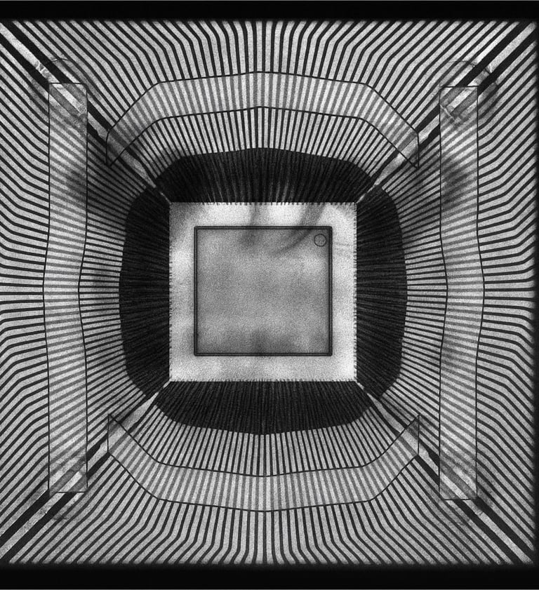
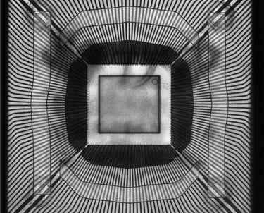
X-ray Analysis
X-ray radiography provides non-destructive insight into internal package structures and interconnect quality without the need for sample cross-sectioning. It is a primary tool for assessing assembly integrity and hidden defects.
Detects opens, voids, shorts, and misalignments in wire bonds and solder joints.
Evaluates die attach coverage and uniformity.
Identifies trapped voids, delamination, or insufficient solder fill in BGAs and QFNs.
Can be configured as 2D radiography or 3D computed tomography (CT) for volumetric imaging.
This technique is invaluable for verifying process quality and for pre-screening samples before destructive analysis.

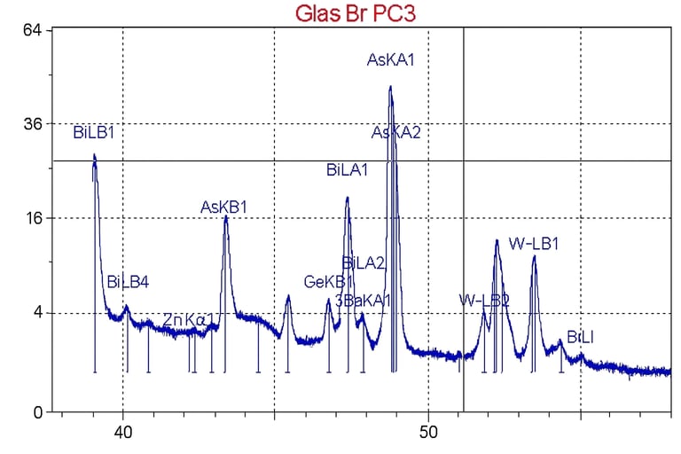
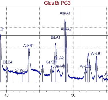
X-ray Fluorescence (XRF)
XRF is used for non-destructive measurement of coating thickness and material composition across various metallization layers. It ensures compliance with plating and lead-finish specifications.
Measures layer thickness and uniformity of Au, Ni, Pd, Sn, and Ag coatings.
Confirms Pb-free and RoHS compliance.
Identifies plating anomalies that may impact solderability or bond reliability.
Provides elemental verification for material traceability.
XRF plays a vital role in process control and reliability verification, particularly for wire bond pads, solder balls, and package terminations.
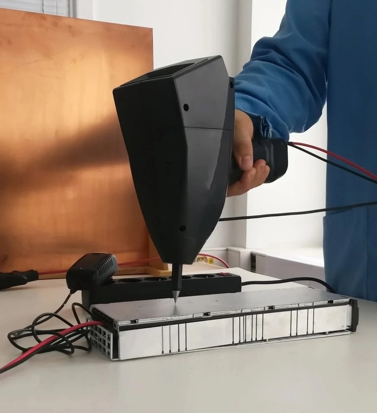
Scanning Acoustic Microscopy (SAM)
SAM utilizes high-frequency ultrasound to detect internal defects, delamination, and voids in packaged devices and die assemblies. It is entirely non-destructive and highly sensitive to interfacial separation.
Evaluates mold compound-to-die, die attach, and substrate interfaces.
Detects delamination, voids, cracks, and blistering.
Supports JEDEC and IPC/JEDEC J-STD-035 acceptance criteria.
Provides acoustic C-scan and through-scan imaging modes.
SAM is essential for verifying package integrity after reliability stresses such as temperature cycling, moisture exposure, or reflow simulation.
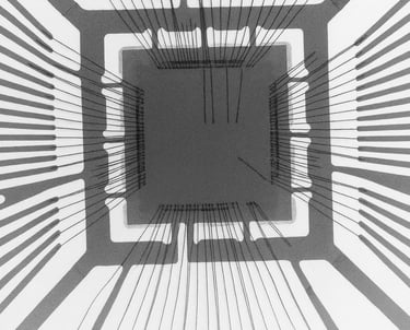
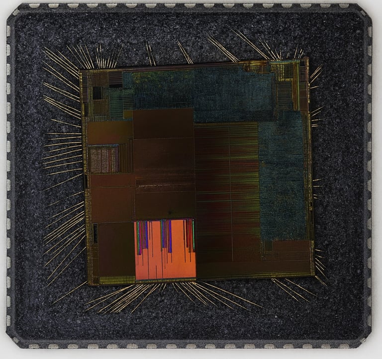
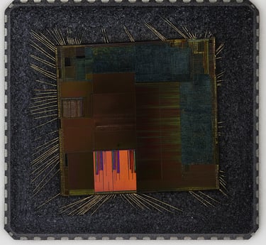
Decapsulation & Die Analysis
Decapsulation is the controlled removal of molding compound or encapsulant to expose the die surface for direct inspection and analysis. It enables detailed evaluation of failure sites and die-level defects.
Uses chemical, plasma, or mixed-mode etching processes depending on wire material.
Reveals passivation damage, corrosion, and metallization failures.
Enables optical, SEM, and EDX examination of die-level anomalies.
Provides access for micro-probing and electrical fault localization.
Die analysis following decapsulation is a critical step in determining root-cause mechanisms such as ESD events, electro-migration, or bond degradation.
Mechanical & Physical Evaluation
Mechanical integrity testing verifies the strength and durability of interconnects, die attach, and encapsulation layers. Through cross-sectioning, thermal hotspot mapping, and detailed visual inspection, we assess physical robustness and identify latent weaknesses that may impact long-term reliability.
Cross-Sectioning
Cross-sectioning (microsectioning) provides a direct, detailed view of the internal structure of a semiconductor package or interconnect system. It is used to examine the integrity of bonds, interfaces, and metallization layers after processing or failure.
Reveals layer interfaces, solder joints, die attach, and wire bond foot formation.
Allows measurement of intermetallic layer thickness, voiding, and delamination.
Supports metallurgical evaluation under optical or SEM imaging.
Enables documentation of mechanical stress or fracture paths.
At Si-Craft Technologies, precision mechanical polishing or focused ion beam (FIB) sectioning is employed depending on the feature size and required resolution. This method is vital for correlating visual or electrical defects with physical root causes, providing permanent records for reliability investigations.
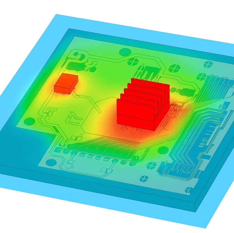
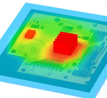
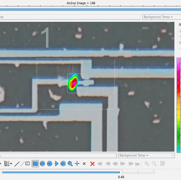
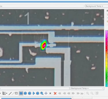
Hot Spot Analysis
Hot Spot Analysis detects localized heating or emission activity caused by electrical shorts, leakage, or junction failures. It uses thermal or photon-based detection to pinpoint failure sites non-destructively.
Employs Infrared (IR) Thermography and Emission Microscopy (EMMI) for high-resolution localization.
Identifies leakage currents, resistive opens, and transient breakdown events.
Detects abnormal thermal gradients in power or analog components.
Enables correlation between physical defect sites and electrical signatures.
Hot Spot Analysis is often an early diagnostic step before decapsulation or cross-sectioning, allowing accurate failure localization without disturbing device structure. It is especially effective for low-level leakage or intermittent faults.
External Visual Inspection
External Visual Inspection is the first line of failure assessment, providing a rapid, standardized evaluation of a component’s physical condition. It helps identify mechanical damage, contamination, and marking discrepancies that may indicate process or handling issues.
Detects package cracks, lead deformation, and surface contamination.
Verifies component marking, polarity, and workmanship quality.
Conducted per MIL-STD-883 Method 2009 and JESD22-B101 visual criteria.
Supports incoming inspection, lot release, and pre-FA screening.
Performed under controlled lighting and magnification, this inspection step ensures that only physically sound samples proceed to deeper analysis. It forms a critical quality gate in both reliability testing and root cause analysis workflows.


Electrical & Functional
Electrical verification ensures devices perform to specification before and after environmental stress. Continuity, resistance, and functional assessments help detect opens, shorts, and degradation mechanisms critical to reliable semiconductor operation.
Continuity and Functional Electrical Testing
Electrical testing validates device integrity and functional performance under standard and stress conditions. It identifies opens, shorts, and marginal behaviors that impact device reliability and end-use performance.
Continuity Testing: Detects open or short circuits at the package or interconnect level.
Parametric Testing: Measures I–V characteristics, leakage, resistance, and threshold levels.
Functional Verification: Confirms device operation according to specification or customer-provided test vectors.
Post-Stress Testing: Evaluates electrical degradation after environmental exposure (HTOL, temperature cycling, HAST).
These tests are essential for correlation between electrical failures and physical mechanisms observed in analytical analysis. Automated test systems and micro-probing tools enable precise fault isolation and correlation with subsequent cross-sectional or die-level investigations.
ESD and Latch-up Evaluation
Electrostatic Discharge (ESD) and Latch-up testing assess a device’s resilience against electrical overstress events that can cause latent or catastrophic damage.
HBM (Human Body Model): Simulates discharge through human contact (JESD22-A114).
MM (Machine Model): Simulates discharge from charged equipment (JESD22-A115).
CDM (Charged Device Model): Tests self-charging events (JESD22-C101).
Latch-up Testing: Detects CMOS parasitic activation and current runaway (JESD78).
Testing ensures device protection circuits, isolation, and substrate design comply with reliability and qualification standards. Results help prevent field failures related to ESD handling or power transients during assembly and operation.
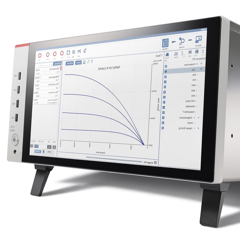
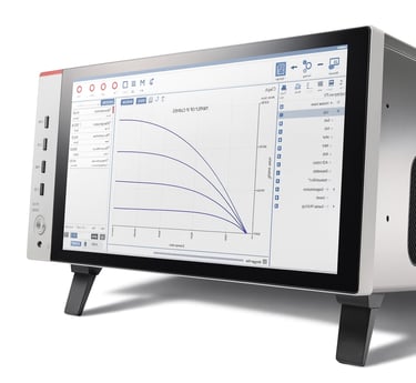
Parametric and Failure Localization Testing
Advanced electrical probing techniques allow precise characterization of failing nodes or regions within a die or package. These tests bridge the gap between system-level symptoms and localized defect mechanisms.
Curve Tracing: Evaluates transistor and junction behavior for leakage or breakdown.
OBIRCH (Optical Beam Induced Resistance Change): Locates resistive defects through thermal or optical response mapping.
Thermal Emission (TIVA): Identifies short circuits via localized heat emission under bias.
Micro-Probing: Provides electrical access to isolated interconnects, enabling node-level analysis.
These methods are critical for correlating electrical signatures with physical damage identified by SEM, SAM, or cross-sectioning, completing the FA workflow from symptom to root cause.